Digital Calculator Chip Design
A 64-bit arithmetic controller implemented in SystemVerilog and verified through Cadence simulation and physical-design tools.
01 // PROJECT OVERVIEW
System design and implementation
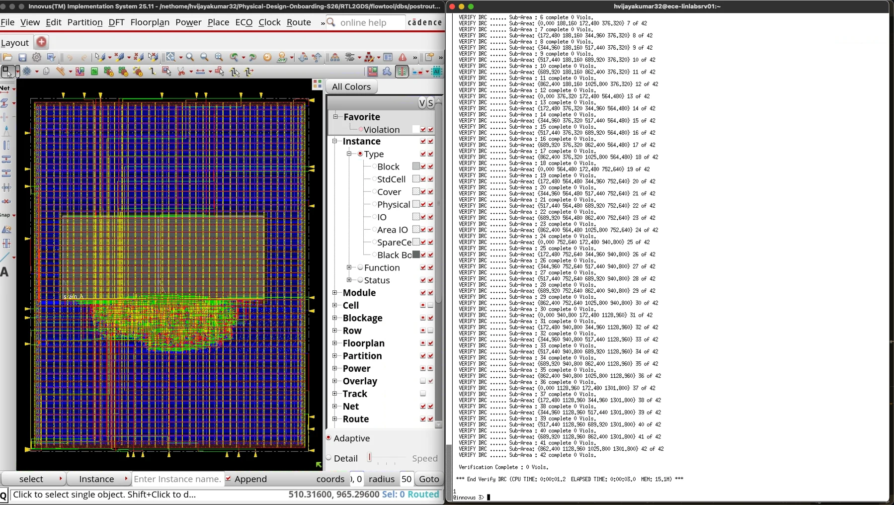
This project followed a digital ASIC design workflow beginning with RTL implementation and functional verification. The arithmetic controller was simulated using Cadence Xcelium and inspected through SimVision before synthesis and physical-design exploration in Cadence Innovus.
ASIC DESIGN FLOW
TECHNICAL HIGHLIGHTS
01
Implemented a 64-bit arithmetic controller in SystemVerilog.
02
Developed testbench logic for functional verification.
03
Analyzed simulation behavior using Xcelium and SimVision.
04
Explored synthesis and physical implementation using Cadence Innovus.
05
Validated arithmetic and SRAM-related behavior through simulation.